Absolute maximum ratings
Maximum ratings are the extreme limits to which the chip can be exposed for a limited amount of time without permanently damaging it. Exposure to absolute maximum ratings for prolonged periods of time may affect the reliability of the device.1
| Note | Min. | Max. | Unit | |
|---|---|---|---|---|
| Supply voltages | ||||
| VDD | -0.3 | +3.9 | V | |
| VDDH | -0.3 | +5.8 | V | |
| VBUS | -0.3 | +5.8 | V | |
| VSS | 0 | V | ||
| I/O pin voltage | ||||
| VI/O, VDD ≤3.6 V | -0.3 | VDD + 0.3 | V | |
| VI/O, VDD >3.6 V | -0.3 | 3.9 | V | |
| NFC antenna pin current | ||||
| INFC1/2 | 80 | mA | ||
| Radio | ||||
| RF input level | 10 | dBm | ||
| Environmental aQFN™73 package | ||||
| Storage temperature | -40 | +125 | °C | |
| MSL | Moisture Sensitivity Level | 2 | ||
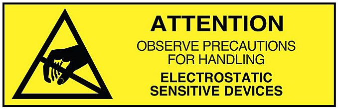
| ESD HBM | Human Body Model | 2 | kV | |
| ESD HBM Class | Human Body Model Class | 2 | ||
| ESD CDM | Charged Device Model | 450 | V | |
| Environmental QFN48 package | ||||
| Storage temperature | -40 | +125 | °C | |
| MSL | Moisture Sensitivity Level | 2 | ||
| ESD HBM | Human Body Model | 4 | kV | |
| ESD HBM Class | Human Body Model Class | 3A | ||
| ESD CDM | Charged Device Model | 1 | kV | |
| Environmental WLCSP 3.544 x 3.607 mm package | ||||
| Storage temperature | -40 | +125 | °C | |
| MSL | Moisture Sensitivity Level | 1 | ||
| ESD HBM | Human Body Model | 1 | kV | |
| ESD HBM Class | Human Body Model Class | 1C | ||
| ESD CDM | Charged Device Model | 500 | V | |
| Flash memory | ||||
| Endurance | 10 000 | write/erase cycles | ||
| Retention at 85 °C | 10 | years | ||