Maximum ratings are the extreme limits to which the chip can be exposed to for a limited amount of time without permanently damaging it. Exposure to absolute maximum ratings for prolonged periods of time may affect the reliability of the device.
| Pin | Note | Min. | Max. | Unit |
|---|---|---|---|---|
| VDD | Supply voltage | 0 | 3.6 | V |
| VSS | Supply voltage | 0 | V | |
| VI/O |
Digital I/O pin voltage VDD ≤ 3.6 V |
-0.3 | VDD + 0.3 | V |
| PIN_TRX |
RF I/O pin input power CW, Transmit mode |
+5 | dBm | |
| PIN_ANT |
RF I/O pin input power CW, Receive/Program mode |
+15 | dBm |
| Note | Min. | Max. | Unit | |
|---|---|---|---|---|
| Storage temperature | -40 | 125 | °C | |
| Reflow soldering temperature | IPC/JEDEC J-STD-020 | 260 | °C | |
| MSL | Moisture sensitivity level 2 | |||
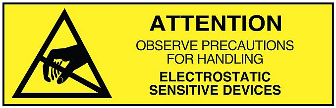
| ESD HBM | Human Body Model | 1 | kV | |
| ESD CDM | Charged Device Model | 2 | kV |